Case studies
Semiconductor
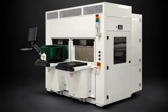
Developing new metrology or inspection technologies for an advanced semiconductor fab is a very complex endeavor requiring specialized knowledge and significant capital expense. A European startup needed…
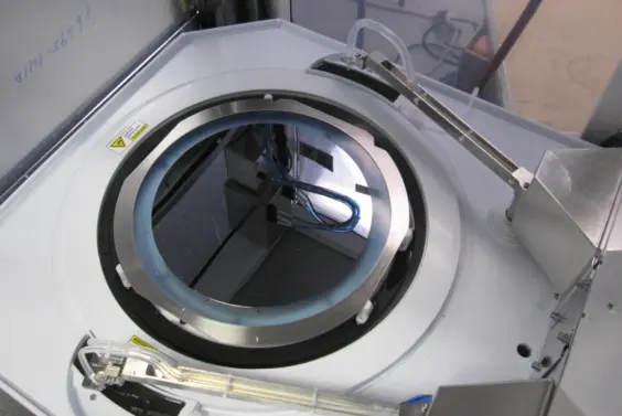
A tier 1 semiconductor OEM needed a custom solution for precise spin coating, cleaning and drying of a special liquid on a wafer mounted on a film frame to enable a downstream process. There were no off-the-shelf…
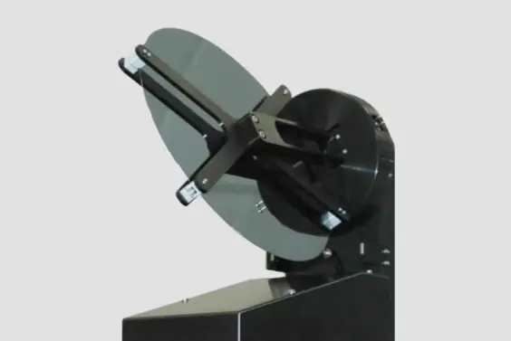
Backside contamination inspection and other process advancements require wafers to be loaded into process or inspection chambers in a 90° or 180° flipped orientation. Adding a wrist to a robot can meet…
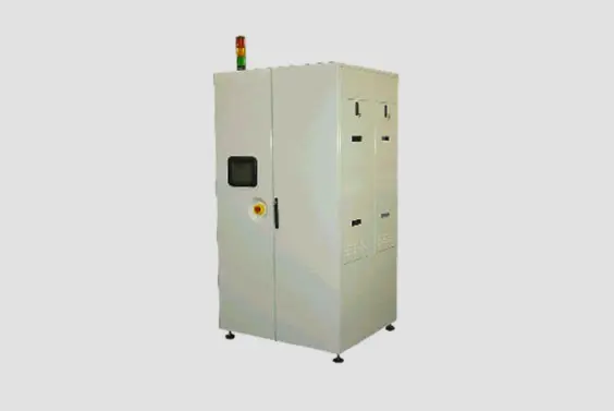
The client needed to upgrade a mature gas waste abatement system while incorporating features from two recently acquired products with different designs and components. Internal engineering resources were…
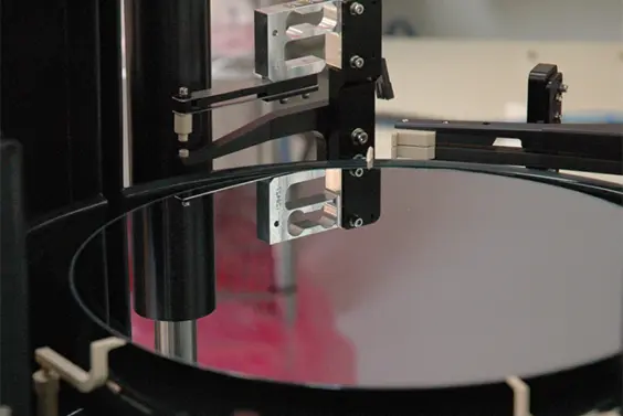
The OEM needed to implement multiple bonding technologies into a small-footprint, wet environment platform. Wafer cleaning, drying, alignment, and joining mechanisms had to be robust, non-particle generating,…
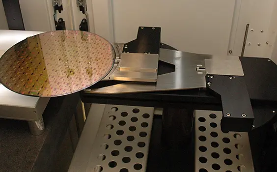
The customer needed to deliver their confocal IR laser scanning technology on a fully automated 300 mm platform. Developing in-house automation would have diverted engineering resources and delayed commercialization….
The MoCVD deposition process is critical to HBLED manufacturing, with tightly constrained carrier pockets and strict no-contact requirements on both wafer sides. Manual loading could not meet throughput…
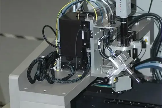
The OEM needed to transition a lab-demonstrated wafer probe process to a production-ready, fully 300 mm-compliant automation platform. The system required micron-level wafer positioning, exceptional positional…
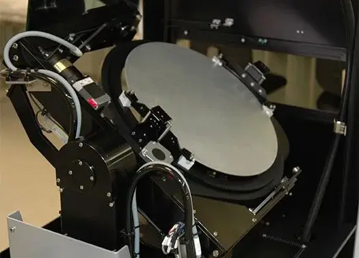
The OEM needed a macro defect inspection module that integrated seamlessly with their wafer sorter. The module had to enable front- and back-side visual inspection under uniform illumination, meet stringent…
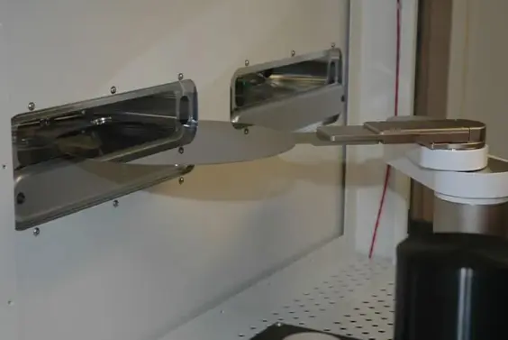
Next-generation process and device technologies demanded new measurement tools, but fabs require fully automated 300 mm configurations for evaluation. Our client needed a high-vacuum wafer automation platform…
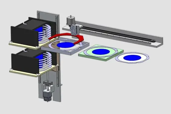
The rapid growth of the HBLED market required laser equipment manufacturers to increase wafer dicing throughput, reduce costs, and replace mechanical dicing technologies. To meet the market window, the…
Our client’s revolutionary CO₂ cleaning technology removes micron and submicron particulate and organic contamination, but to be evaluated by a leading-edge fab, it needed to be implemented on a fully…