Commercializing semiconductor metrology and inspection lab-to-fab technologies
Developing new metrology and inspection technologies for an advanced semiconductor fab is a complex task that needs specialized knowledge and significant capital investment. AIR minimizes development cost and risk to bring these systems to market by providing a fab-ready, customizable system platform and complete manufacturing infrastructure to support high-volume manufacturing (HVM) scaling. This includes change management, configuration management, reliability, and cost reduction.
Capabilities
Accelerating your time to market with a global leader in metrology and inspection
AIR has integrated more metrology and inspection technology systems for leading semiconductor OEMs than any other engineering firm worldwide. We design and build fab-ready prototypes that often go directly into semiconductor fabs, accelerating your time to market.
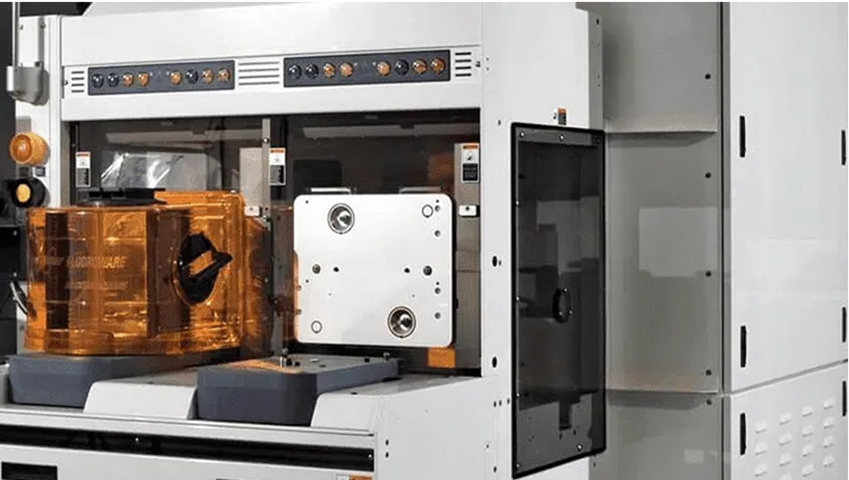
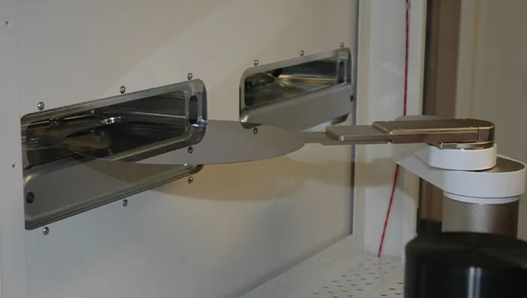
- Wafer handling systems with customized configurationsIncluding EFEM, FOUP and SMIF interfaces, wafer identification, and support for all substrate types and sizes — from thinned wafers and unusual form factors to silicon, SiC, GaN, glass/ceramic, III-V and II-VI materials, as well as film frames, packages, printed circuit boards (PCBs), and masks, using vacuum, edge-grip, flipping and non-contact end effectors.
- Precision wafer stage systemsDelivered as custom developments or integrated third-party solutions, offering sub-micron accuracy with mechanical or air-bearing stages, linear or rotary scanning, high-vacuum compatibility, customized chuck design, backside contamination control, and micron-level flatness and leveling.
- Controlled environmentsDesigned to operate in ISO Class 1 and ISO Class 3 cleanrooms with customer-validated mechanisms, incorporating vibration and acoustic noise isolation, and precise control of temperature, vacuum, humidity, oxygen levels, magnetic fields, and light-tight conditions.
- Process integrationCovering full tool-level integration of metrology and inspection processes, including precision motion, inspection technologies, automation sequencing, and reliable interfacing with upstream and downstream semiconductor manufacturing equipment.
- Standards complianceEFEM and SECS/GEM integration, ensuring compatibility with semiconductor manufacturing standards through robust EFEM design, SECS/GEM communications, equipment control, data exchange, and factory automation integration.
Approach
Bring your inspection and metrology technologies to market faster
We develop fully custom inspection and metrology systems or integrate your proprietary technology into our proven, semi-custom platform. Our expertise spans wafer handling, precision motion stages, and environmental controls, supporting everything from manual-load configurations to fully automated systems.
- 600+ production systems shipped since 2003AIR has developed more than 25 product lines for startups to tier-1 semiconductor OEMs, and shipped over 600 production systems worldwide.
- Complete custom solutionsWe partner with OEMs from concept development to prototype build to HVM.
- Direct-to-end-customer shipping optionMany systems are fully tested at AIR and drop-shipped directly to the semiconductor end customer.
- AdditionallyWe support modular and scalable system architectures, serviceability-focused design, and automation platforms engineered for repeatable deployment, future expansion, and long-term production reliability.
Impact
Accelerating lab-to-fab transition for semiconductor metrology and inspection
Our metrology and inspection solutions enable our customers to achieve more, more quickly, with less risk, and often at a lower cost.
- Cut your time-to-marketDeveloping metrology and inspection technology requires a different skill set than semiconductor equipment design. We offer a pre-engineered system that needs only minimal customization. With pre-negotiated module delivery and streamlined manufacturing, it enables fast, efficient integration and testing, so you can quickly transform your innovation into a production-ready system.
- Reduce engineering costsOur pre-engineered system architecture features modular interfaces across software, mechanical, and electrical systems, which can significantly reduce your engineering costs.
- Accelerate and streamline early-stage validation and your path to manufactureThe R&D version of our platform offers a clean, compliant enclosure with manual wafer loading, ideal for customer-site demonstrations and process qualification. As your product evolves, the same system can be upgraded to HVM for fully automated wafer handling and factory integration, all without altering your process hardware. This seamless upgrade path ensures process consistency from R&D to HVM.
- Free up your development teamOur platform manages wafer handling and recipe editing with precision. It controls the transfer of wafers from front-opening unified pods (FOUPs) or cassettes, aligns and maps them, and positions them accurately on the chuck. While your metrology and inspection system captures wafer data, the orchestrator manages communication, transmitting data back to the fab using standard SECS/GEM protocols. After processing, the integrated EFEM robot returns each wafer to its designated slot. By handling the factory interface and automation, our platform frees up your team, allowing them to focus on advancing your core technology.
- Reduce riskOur platform minimizes adoption barriers by incorporating widely recognized OEM components already trusted in semiconductor fabs.
Case studies
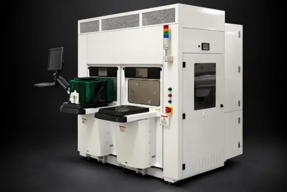
Developing new metrology or inspection technologies for an advanced semiconductor fab is a very complex endeavor requiring specialized knowledge and significant capital expense. A European startup needed…
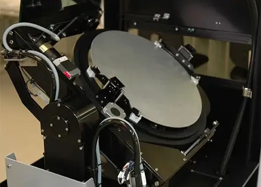
The OEM needed a macro defect inspection module that integrated seamlessly with their wafer sorter. The module had to enable front- and back-side visual inspection under uniform illumination, meet stringent…
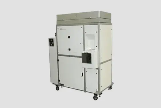
Candela Instruments had proven their optical surface scanning technology on a manually loaded machine, but expanding to full production required a fully automated, in-line system. The automation had to…