Reducing product development cycles for semiconductor metrology and inspection
Project snapshot
Client:
Location:
Sector:
Product type:
Challenge
Successfully bring a startup OEM’s innovative technology to market on an accelerated schedule
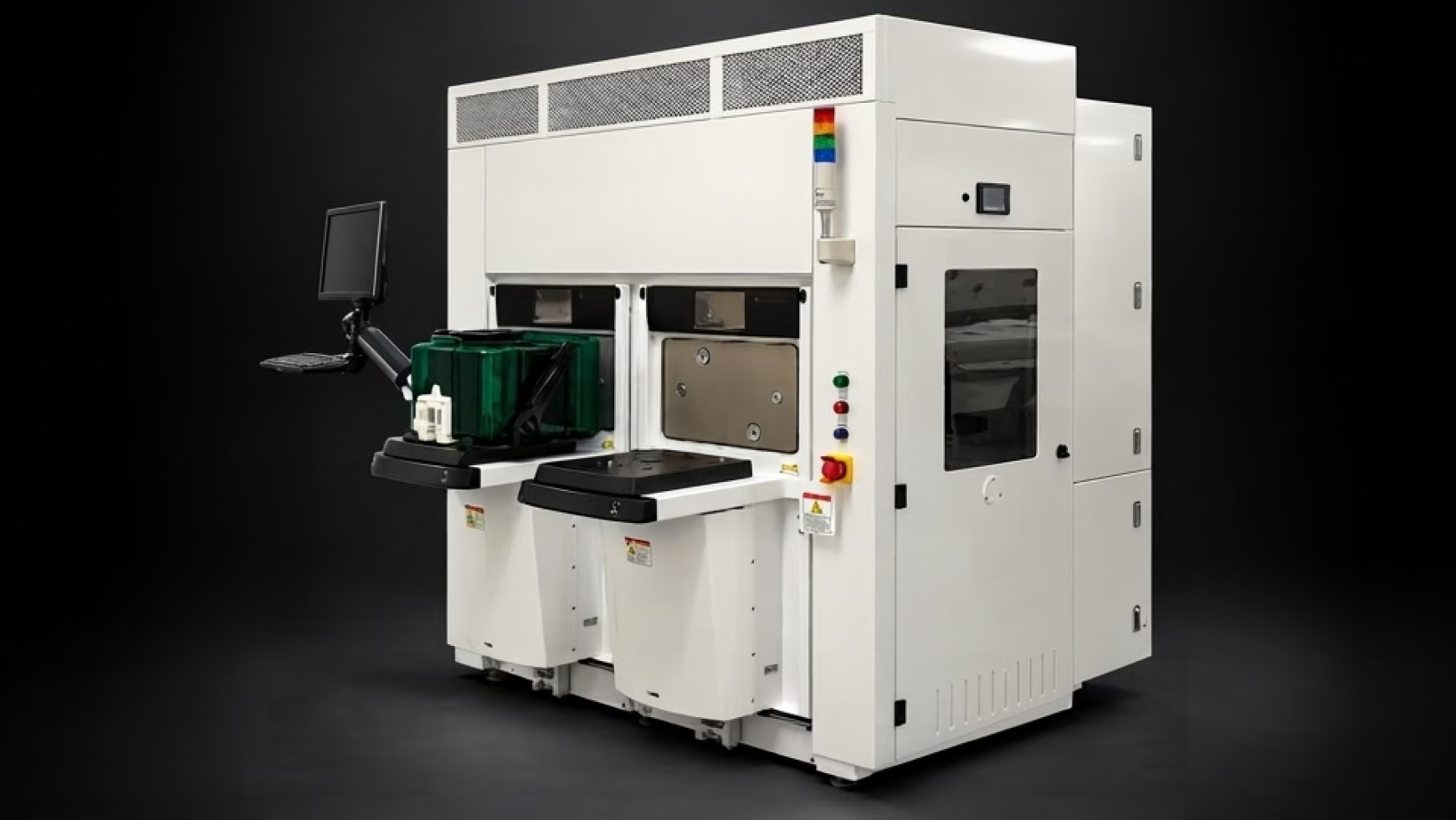
Developing new metrology or inspection technologies for an advanced semiconductor fab is a very complex endeavor requiring specialized knowledge and significant capital expense. A European startup needed to rapidly transform their R&D lab based tool to a fully automated, reliable FAB-ready system that was fully compliant with semiconductor industry standards and semiconductor fab common specifications.
Innovation
Leveraged semi-custom platform to quickly deliver their R&D to fabs world-wide
AIR integrated the OEM’s unique metrology and inspection technology into a fully custom platform including wafer handling, high accuracy staging, and environmental controls and software to create an automated, FAB ready system. Our deep expertise reduced the development cost, risk and timeline to develop the complex system. AIR also provided a complete manufacturing infrastructure for on-going system manufacturing including changes, configuration management, reliability, and cost reduction.
The result was a customized platform to meet the specific requirements of our customer’s measurement technology. The platform included wafer handling, staging, contamination and environment control, integration of our customer’s measurement sub-system, and final system test and shipment.
AIR’s capabilities included:
- Wafer handling system and manage special configurations
- EFEM, FOUP, SMIF, Wafer ID
- All substrate types & sizes, thinned wafers, unusual form factors
- All end effector types, vacuum, edge, flipping, non-contact
- Develop or integrate third party wafer staging system
- High precision (sub-micron), air bearing, linear or rotary scanning, vacuum
- Customized platen design, backside contamination control
- Environmental control systems
- Vibration control (passive & active), clean air (ISO Class 1), cleanliness, temperature, light
- Integrate measurement sub-system
- Optical, electrical, magnetic, related data acquisition and processing sub-systems
- System Software, HMI, Calibration, Maintenance Utilities and Field Support Documentation
- Full system integration, testing, configuration management, and drop shipment to end-user fab
- Regulatory compliance (Semi, I300I, CE)
Result
Built a fully automated, reliable FAB-ready system in a shorter timeframe
Our deep industry experience and understanding of the needs of end customers helped the team rapidly transform their R&D lab designed technology to a fully automated, reliable FAB-ready system that was fully compliant with standards for the semiconductor industry. We achieved significant reduction in end customers’ product development cycles.
By successfully bringing innovative technology to market fast, we helped the company quickly become a market leader, strategically positioning the company for acquisition by KLA in 2019.
Featured capabilities:
Featured sectors:
Case studies
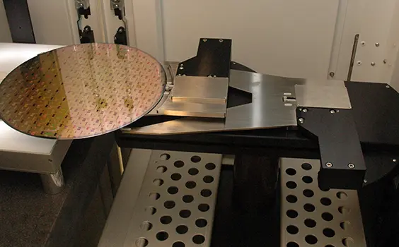
The customer needed to deliver their confocal IR laser scanning technology on a fully automated 300 mm platform. Developing in-house automation would have diverted engineering resources and delayed commercialization….
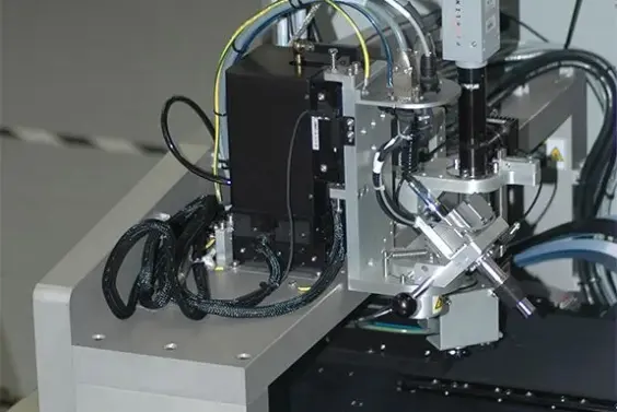
The OEM needed to transition a lab-demonstrated wafer probe process to a production-ready, fully 300 mm-compliant automation platform. The system required micron-level wafer positioning, exceptional positional…
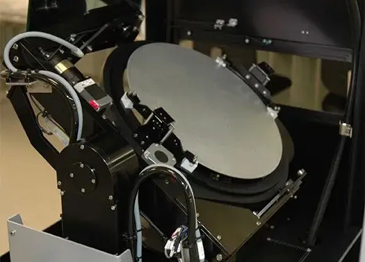
The OEM needed a macro defect inspection module that integrated seamlessly with their wafer sorter. The module had to enable front- and back-side visual inspection under uniform illumination, meet stringent…