Fully automated 300 mm platform for bonded wafer metrology and defect review
Project snapshot
Client:
Location:
Sector:
Product type:
Challenge
Enable precision 3D metrology for bonded wafers without diverting critical R&D resources
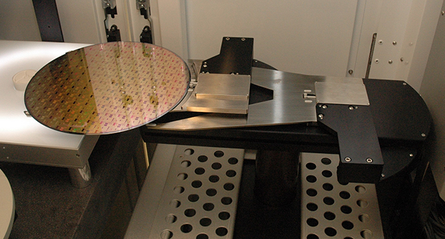
The customer needed to deliver their confocal IR laser scanning technology on a fully automated 300 mm platform. Developing in-house automation would have diverted engineering resources and delayed commercialization. The system had to handle fragile bonded wafers, integrate vibration isolation, maintain clean airflow, and comply with SEMI safety and automation standards.
Innovation
Custom wafer handling and metrology integration for warped bonded wafers
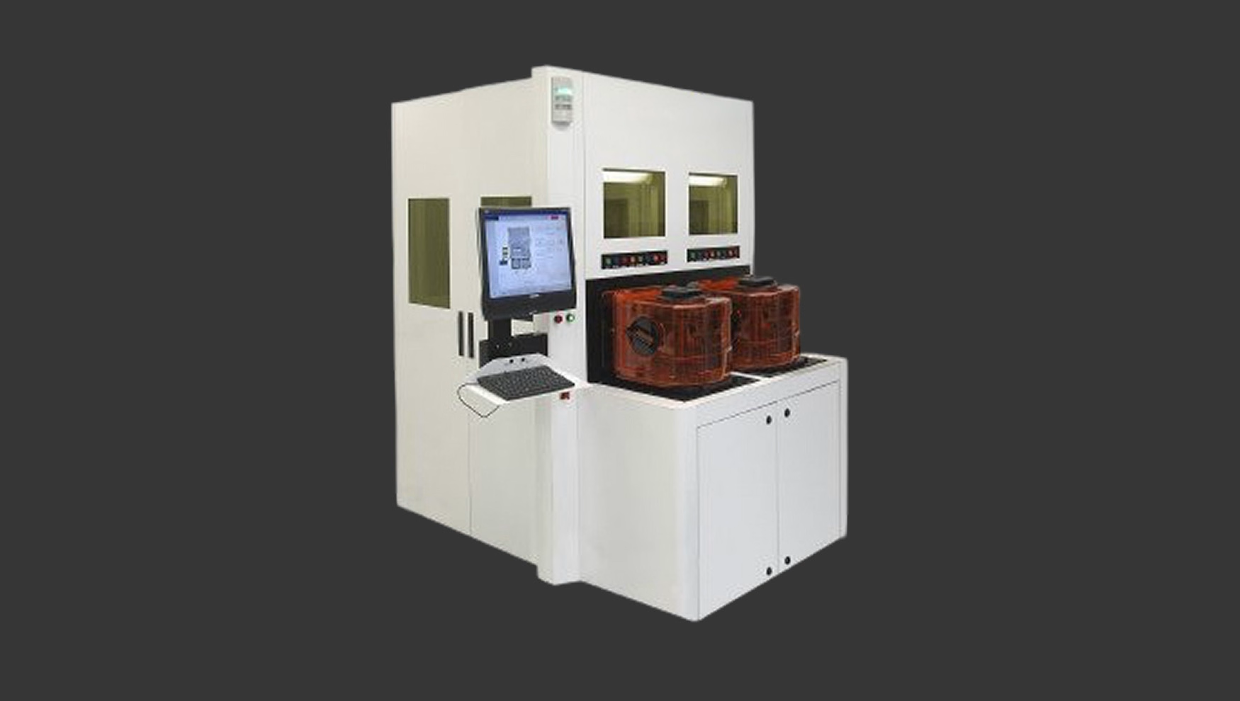
We partnered closely with the customer to design a system that included:
- Precision staging and robotic wafer handling for accurate positioning.
- Innovative mechanisms to accommodate severely warped bonded wafers.
- Vibration isolation and clean airflow for measurement accuracy.
- Load ports, system framing, and full compliance with SEMI safety and factory automation standards.
- Integration of confocal IR laser scanning for 3D imaging, thickness measurement, and defect review.
Result
Rapid deployment of a fully automated metrology platform
The platform enabled high-precision 3D bonded wafer inspection while allowing the customer to remain focused on their core technology. The system met automation, safety, and performance requirements, supporting rapid adoption by customers in the 3D IC market.
Featured capabilities:
Featured sectors:
Case studies
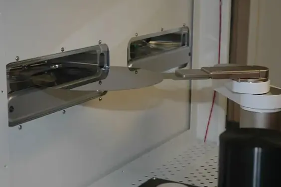
Next-generation process and device technologies demanded new measurement tools, but fabs require fully automated 300 mm configurations for evaluation. Our client needed a high-vacuum wafer automation platform…
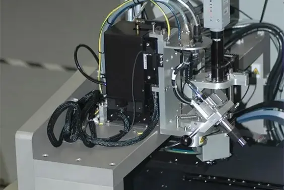
The OEM needed to transition a lab-demonstrated wafer probe process to a production-ready, fully 300 mm-compliant automation platform. The system required micron-level wafer positioning, exceptional positional…
Attolight, a European startup, needed to rapidly scale their electron-beam lab tool into a semiconductor fab-ready system to meet customer requirements. The project presented multiple challenges: