Fully automated 300 mm wafer CO₂ cleaning platform
Project snapshot
Client:
Location:
Sector:
Product type:
Challenge
Implement a fully automated 300 mm platform for next-generation CO₂ cleaning
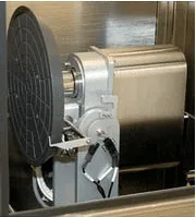
Our client’s revolutionary CO₂ cleaning technology removes micron and submicron particulate and organic contamination, but to be evaluated by a leading-edge fab, it needed to be implemented on a fully automated 300 mm wafer platform. Achieving this required precise control of CO₂ flow, nozzle performance, and particulate removal, as well as extensive airflow modeling to ensure the highest cleanliness levels.
Innovation
Multi-axis automation integrated with advanced CO₂ process controls
We developed the multi-axis wafer stage, CO₂ delivery and nozzle controls, and cleaning chamber in close collaboration with the client’s computational fluid dynamics engineers. Key design features included:
- Optimized cleaning chamber geometry to maximize particulate removal.
- Precise CO₂ pressure and flow management to generate the required solid “snow” stream.
- Integration of an industry-standard EFEM with custom wafer staging for 300 mm wafers.
- Detailed system layout including frame, enclosure, and power systems designed for high throughput and reliability.
- Extensive testing and tuning to balance CO₂ pressures while maintaining maximum cleaning performance.
Result
High-performance automated CO₂ cleaning for leading-edge fabs
The resulting system successfully integrated our client’s novel CO₂ cleaning process into a fully automated 300 mm platform. It achieved the desired particulate removal efficiency and was ready for deployment in advanced semiconductor production environments.
Featured capabilities:
Featured sectors:
Case studies
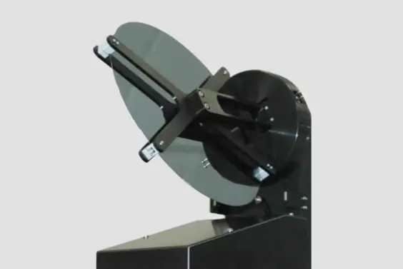
Backside contamination inspection and other process advancements require wafers to be loaded into process or inspection chambers in a 90° or 180° flipped orientation. Adding a wrist to a robot can meet…
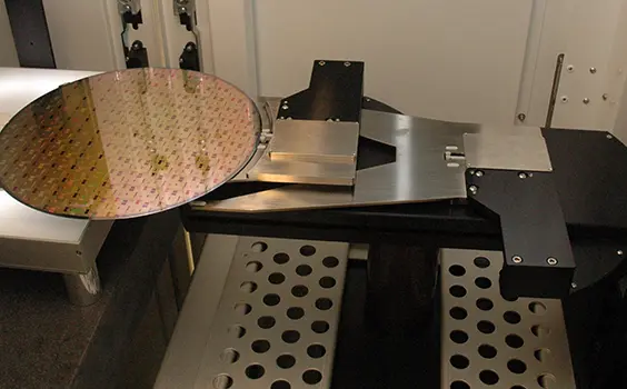
The customer needed to deliver their confocal IR laser scanning technology on a fully automated 300 mm platform. Developing in-house automation would have diverted engineering resources and delayed commercialization….
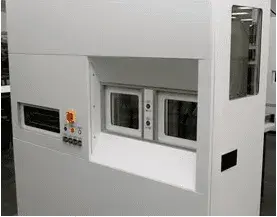
The MoCVD deposition process is critical to HBLED manufacturing, with tightly constrained carrier pockets and strict no-contact requirements on both wafer sides. Manual loading could not meet throughput…