Semiconductor capital equipment that lets you focus on your core technology
Innovation wins markets, but commercialization determines who becomes the market leader. Whether you’re an emerging startup or an established semiconductor OEM developing a next-generation platform, success depends on transforming breakthrough technology into reliable, manufacturable equipment — quickly and with minimal risk. AIR brings the engineering expertise, semiconductor equipment experience, advanced manufacturing capabilities, and commercialization know-how to help customers accelerate development, avoid costly delays, and bring new technologies to market faster.
Capabilities
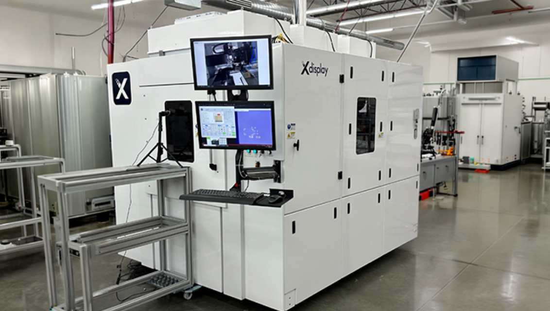
Complex, custom semiconductor capital equipment
AIR specializes in the development of highly complex, custom semiconductor capital equipment where there’s no existing blueprint to follow. For decades we’ve helped innovators succeed with technically demanding, first-of-a-kind projects — solving complex engineering challenges, managing technical uncertainty, and delivering reliable equipment that performs in the world’s most demanding fabs. Our capabilities include:
- Process chambersPVD, PECVD, MOCVD, e-beam litho, nano-imprint, vac dry, plasma metrology, cathodoluminescence, UV processing, transfer modules/load locks, wet clean, Marangoni dry, electrochemical processing
- Substrates200mm wafer, 300mm wafer, film frame, packages, PCBs, masks
- Process environmentsVacuum (down to UHV), atmospheric, inert (+/-15mbar)
- Specification complianceSEMI (S2/S8, etc.), CE mark, customer ‘common spec,’ NFPA 79
- Fab communicationSECS/GEM factory interface integration
- Fab accepted brandsEFEMs, controls, fittings, electronics
- Sensors/controlsTemperature stability, vac level, humidity, O2, B-field, static charge
- Precision motion<5µm position repeatability
- Takt optimizationChamber and system level
- Control systems and softwareDeep understanding of controls architecture, standards and tools
Approach
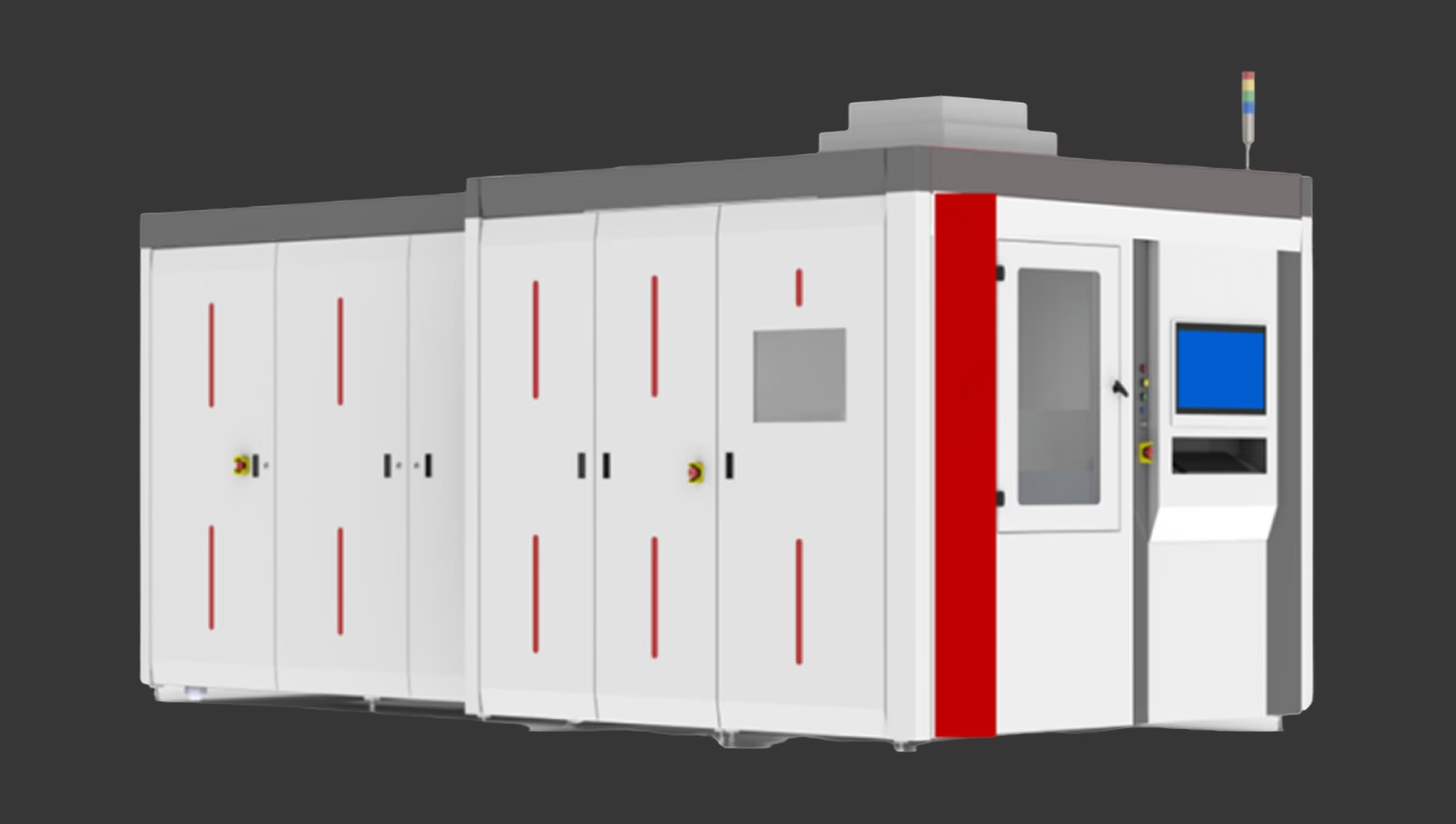
Let us understand your semiconductor capital equipment needs and build you the best solution
Our team includes seasoned engineers, program managers, and technical leaders who built their careers at Silicon Valley’s premier semiconductor equipment companies. We integrate seamlessly with your engineering organization, protecting your intellectual property and keeping proprietary secrets safe, while becoming an extension of your team. Through early business and technical alignment, collaborative concept development, and disciplined project execution, we help identify risks before engineering begins, accelerate decision making, and create a stronger foundation for successful commercialization.
- Substrate type and size
- In-line or off-line process
- Process environment: atmospheric or vacuum
- Service/maintenance items: sparable or consumable
- Sensitivity to vibration
- Sensitivity to temperature fluctuations
- Materials compatibility with process
Impact
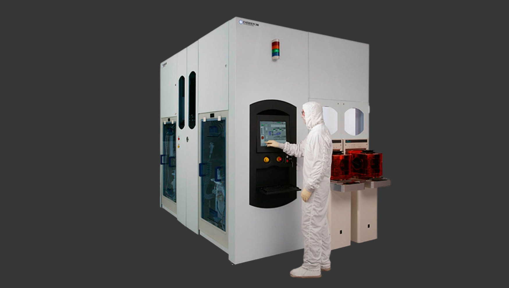
Get to market faster and safer with an instant-on semiconductor development team from AIR
AIR gives you immediate access to a multidisciplinary team with decades of experience designing and delivering complex semiconductor capital equipment. This allows you to accelerate development without the time, cost, and risk of building those capabilities internally. We provide the expertise, execution, and capacity to help you achieve your goals faster. Our customers benefit from reduced technical risk, shorter development cycles, and a trusted partner capable of moving innovative technologies from concept to commercial success.
- Custom solutions developed by AIR belong to you
- Firewalls and isolated network folders keep your information safe
- Physical walls and locked rooms are available to isolate your systems from view
- Reduce your development time by months or quarters by leveraging an instant-on team
- AIR global manufacturing sites enable manufacturing in the US and Europe
Case studies
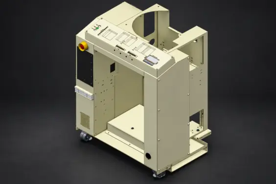
The customer needed a 30% reduction in tool cost while implementing improvements in process technology. The effort had to be low-risk, ensuring no process-critical components were affected, and the first…
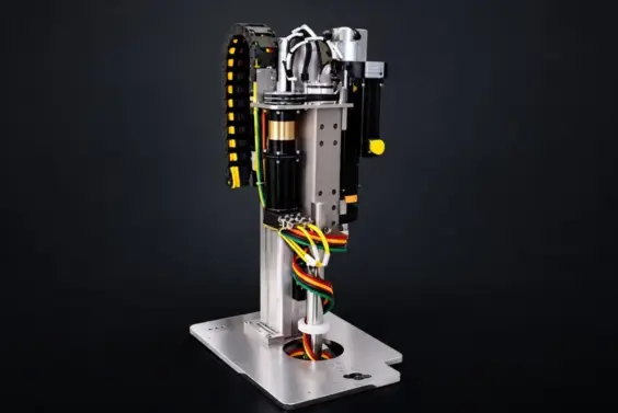
The CMP equipment manufacturer needed a wafer load station to interface with their polishing process. The first design partner failed to deliver, leaving the schedule nearly exhausted and no usable design….
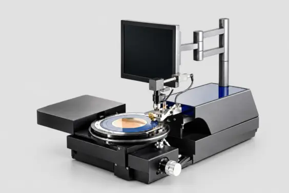
A pioneer in manual wafer scribing and dicing needed to scale their process from 4" to 8" wafers. Their unique approach required the wafer to “float” so that scribing could be accurate and breakage…