Automated wafer loading for high-brightness LED MoCVD carriers
Project snapshot
Client:
Location:
Sector:
Product type:
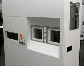
Challenge
Automate precise, non-contact wafer loading for HBLED deposition
The MoCVD deposition process is critical to HBLED manufacturing, with tightly constrained carrier pockets and strict no-contact requirements on both wafer sides. Manual loading could not meet throughput demands or ensure consistent placement. Automation needed to achieve perfect alignment without touching the wafer surfaces while maintaining carrier integrity.
Innovation
Precision Bernoulli-based wafer transfer with vision guidance
We developed a fully automated cassette loading and wafer transfer system leveraging:
- A custom Bernoulli end effector to hold wafers without front or backside contact.
- Machine vision for precise alignment within the tight carrier pockets.
- High-precision mechanics to ensure repeatable, accurate placement.
- Integration with existing HBLED MoCVD carriers without any modification.
Result
Reliable, high-throughput HBLED wafer handling
The automation system successfully delivered non-contact, precision wafer loading, enabling higher throughput and consistent deposition quality for larger HBLED wafers. The solution reduced manual labor and safeguarded critical carrier and wafer integrity.
Featured capabilities:
Featured sectors:
Case studies
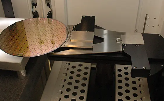
The customer needed to deliver their confocal IR laser scanning technology on a fully automated 300 mm platform. Developing in-house automation would have diverted engineering resources and delayed commercialization….
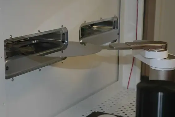
Next-generation process and device technologies demanded new measurement tools, but fabs require fully automated 300 mm configurations for evaluation. Our client needed a high-vacuum wafer automation platform…
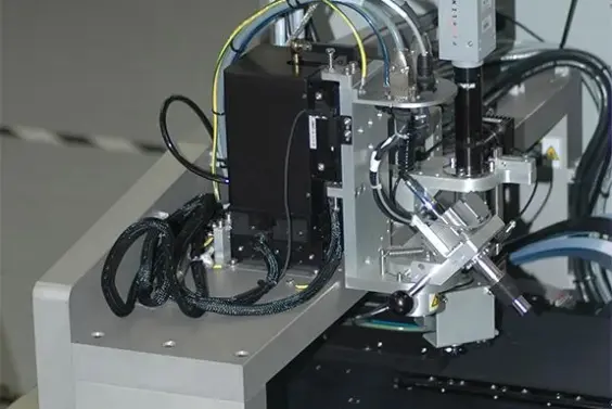
The OEM needed to transition a lab-demonstrated wafer probe process to a production-ready, fully 300 mm-compliant automation platform. The system required micron-level wafer positioning, exceptional positional…