An industry-leading wafer flipper module for advanced semiconductor manufacturing
Challenge
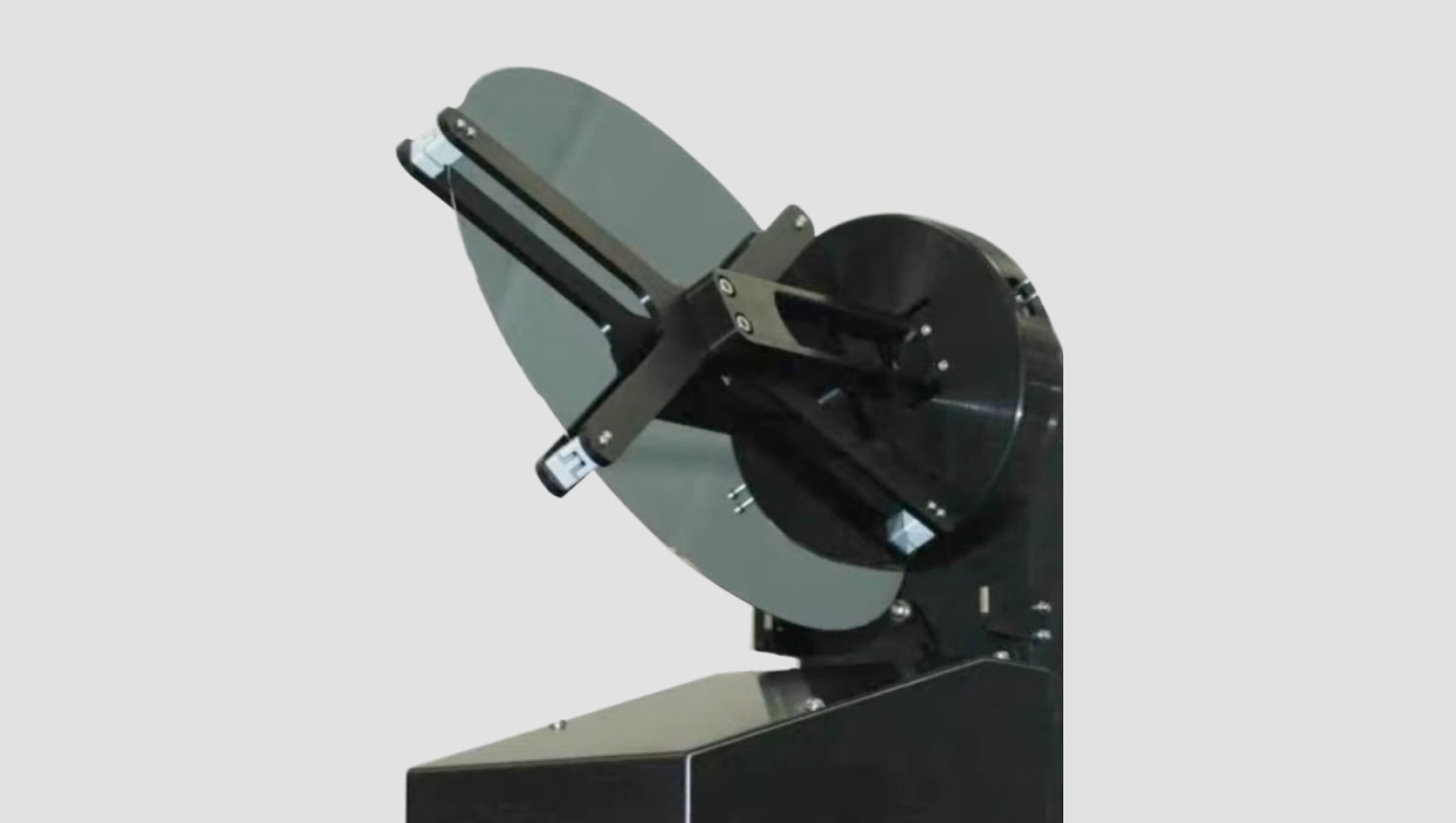
Develop a wafer flipper that could quickly, accurately, and reliably orient the substrate
Backside contamination inspection and other process advancements require wafers to be loaded into process or inspection chambers in a 90° or 180° flipped orientation. Adding a wrist to a robot can meet these needs, but it may reduce throughput and complicate system architecture. The customer tasked us with designing a robust, compact wafer flipper module that could quickly, accurately, and reliably orient the substrate.
Innovation
An adaptable, flexible wafer flipper module
We developed a robust, compact wafer flipper module that quickly, accurately, and reliably orients the substrate. It was designed with the following features:
- Handles both 200mm and 300mm wafers.
- Accurately orients the substrate in a quickly, accurately and reliably.
- Compatible with both edge grip and vacuum paddle end effectors.
- Gripping pads designed with a 3-degree slope to ensure that a 1mm wafer edge exclusion zone is not exceeded.
- Sensors used to detect both wafer presence and wafer grip to guarantee correct wafer placement.
- Designed such that no particles greater than 0.1 µm are detectable coming from the wafer flipper during motion.
- All motors and motion mechanisms contained in a purged enclosure to eliminate any potential particle contamination during the wafer flipping process.
- Designed to easily integrate into existing tool platforms.
Result
Industry-leading tool with excellent performance parameters and a low cost of ownership
AIR has what customers need – a unique, successful wafer flipper that easily integrates into an existing platform. With a small footprint, high level of control, low power requirements, design for ease of maintenance, and compliance with standard regulatory requirements (CE, SEMI, NFPA, ergonomic).
Featured capabilities:
Featured sectors:
Case studies
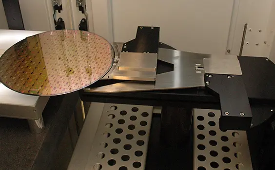
The customer needed to deliver their confocal IR laser scanning technology on a fully automated 300 mm platform. Developing in-house automation would have diverted engineering resources and delayed commercialization….
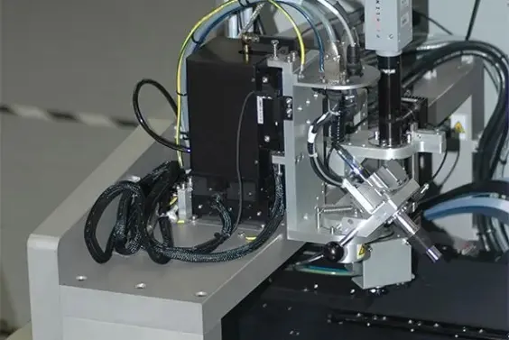
The OEM needed to transition a lab-demonstrated wafer probe process to a production-ready, fully 300 mm-compliant automation platform. The system required micron-level wafer positioning, exceptional positional…
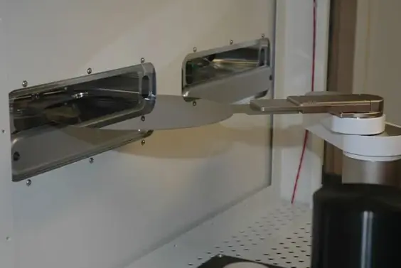
Next-generation process and device technologies demanded new measurement tools, but fabs require fully automated 300 mm configurations for evaluation. Our client needed a high-vacuum wafer automation platform…