Accelerating semiconductor equipment from breakthrough technology to fab-ready production
AIR enables startups, global semiconductor equipment OEMs, and semiconductor fabs to transform next-generation technologies to high-volume production systems on accelerated schedules. With deep expertise in inspection, metrology, wafer processing, and advanced handling systems, we deliver complex semiconductor engineering solutions built on more than four decades of innovation — including 25 years successfully serving semiconductor capital equipment customers in the heart of Silicon Valley.
Why AIR for semiconductor
Accelerate commercialization. Reduce risk.
Deep engineering expertise and collaborative partnership from prototype through production.
AIR accelerates next generation technologies for semiconductor equipment manufacturers while reducing development risk, shortening time to market, and scaling global production with confidence. Combining decades of semiconductor expertise with proven custom and modular platforms, we deliver reliable products ready for production, without sacrificing quality or speed.
Semiconductor capabilities
Semiconductor product and process experience
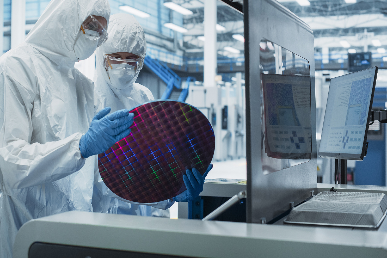
AIR brings deep expertise across semiconductor inspection, metrology, wafer processing, and advanced substrate handling for the largest fabs globally. We engineer the precision manufacturing systems and controlled micro-environments that enable fragile wafers and proprietary semiconductor technologies to perform reliably at scale. With decades of experience commercializing customer innovations, we design equipment that meets the industry’s most demanding standards for precision, cleanliness, reliability, serviceability, and high-volume manufacturing. Our team includes engineers from leading semiconductor OEMs with deep expertise in designing production-ready equipment.


Semiconductor manufacturing capabilities
Technical expertise
Certified excellence
- SECS/GEM factory interface integration
- Standards compliance: SEMI S2, S8 and CE Mark
- ISO class 7 cleanroom assembly and test
- ATEX & high-temperature environments 200°C+
- Sealed inert environments
Sites
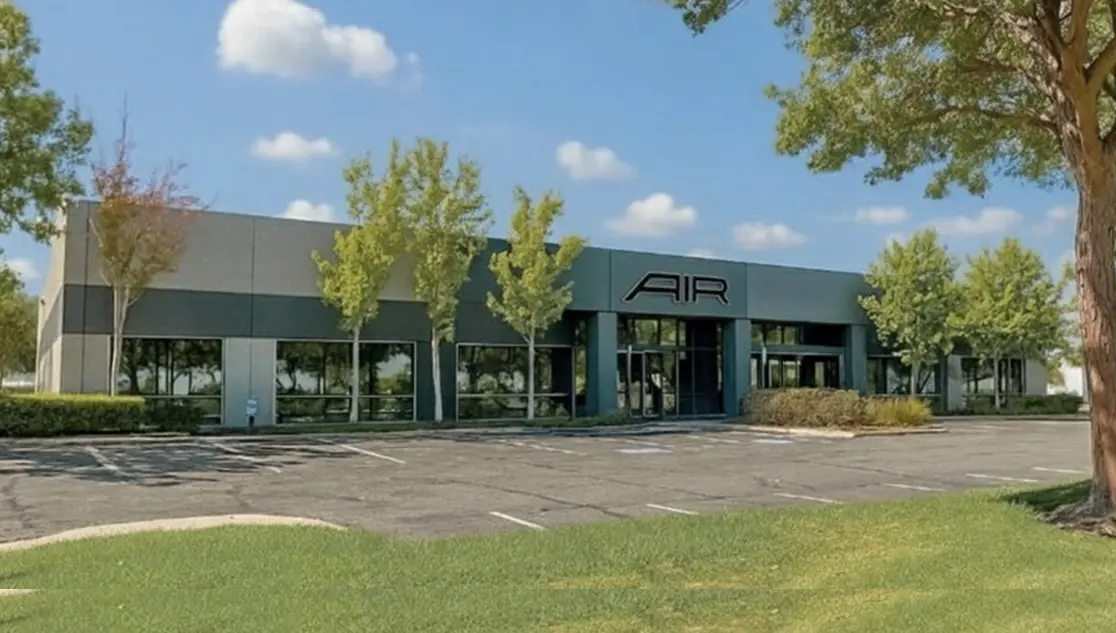
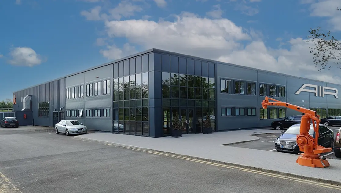
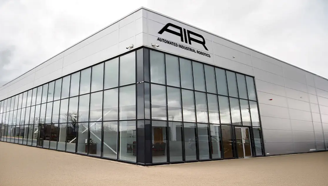
Semiconductor case studies
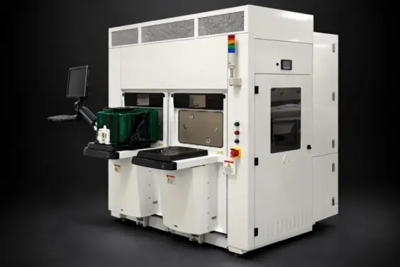
Developing new metrology or inspection technologies for an advanced semiconductor fab is a very complex endeavor requiring specialized knowledge and significant capital expense. A European startup needed…
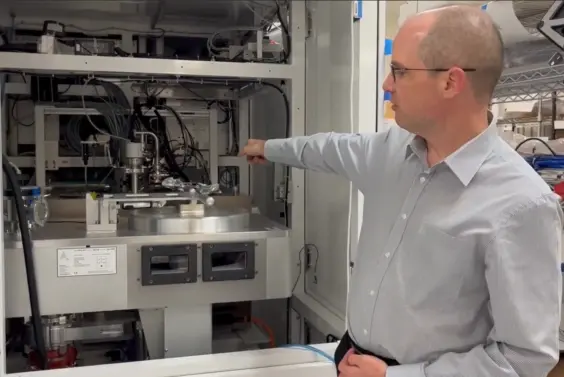
Attolight, a European startup, needed to rapidly scale their electron-beam lab tool into a semiconductor fab-ready system to meet customer requirements. The project presented multiple challenges:
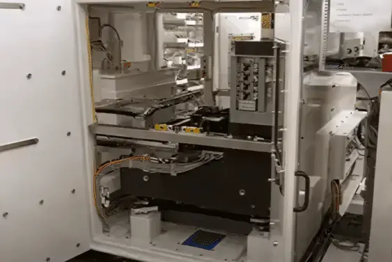
Semiconductor startup Silicon Valley X-Ray (SVXR) had proven its X-ray inspection technology on a laboratory tool and needed to rapidly deliver a production-worthy system for installation in a customer…
Insights
Innovating the future of semiconductor engineering
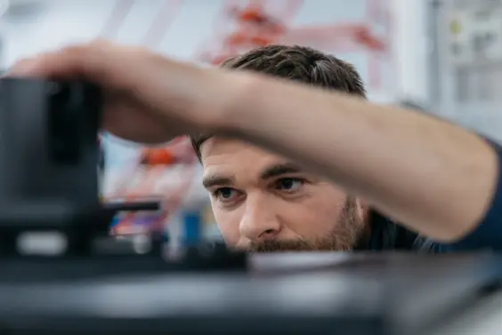
A Proven Approach for Semiconductor OEM Equipment Development
Recent semiconductor projects
OLED display process module
Stacked UV LED curing modules engineered for particle-free, high-volume OLED manufacturing, enabling on-time startup of a $4B display fab and rapid commercialization of flexible OLED technology.
X-ray inspection tool
Transformed a laboratory X-ray prototype into a fab-ready production tool in just months, helping create a new high-speed semiconductor inspection category.
Micro-transfer printing tools
End-to-end design and manufacturing partnership that scaled specialized micro-transfer printing tools while allowing the customer to stay focused on R&D.
Wafer heating & cooling module
High-uniformity thermal management modules delivering rapid heating, cooling, ultra-low contamination, and production-proven reliability.
FOUP load port
Brand-agnostic 300 mm load port delivering interoperability, 40%+ cost reduction, and twice the MTBF target.