Rapid cost-reduced vacuum wafer transfer robot delivered in 10 weeks
Project snapshot
Client:
Location:
Sector:
Product type:
Challenge
Rapidly redesign a vacuum wafer robot to reduce cost while meeting a 10-week evaluation deadline
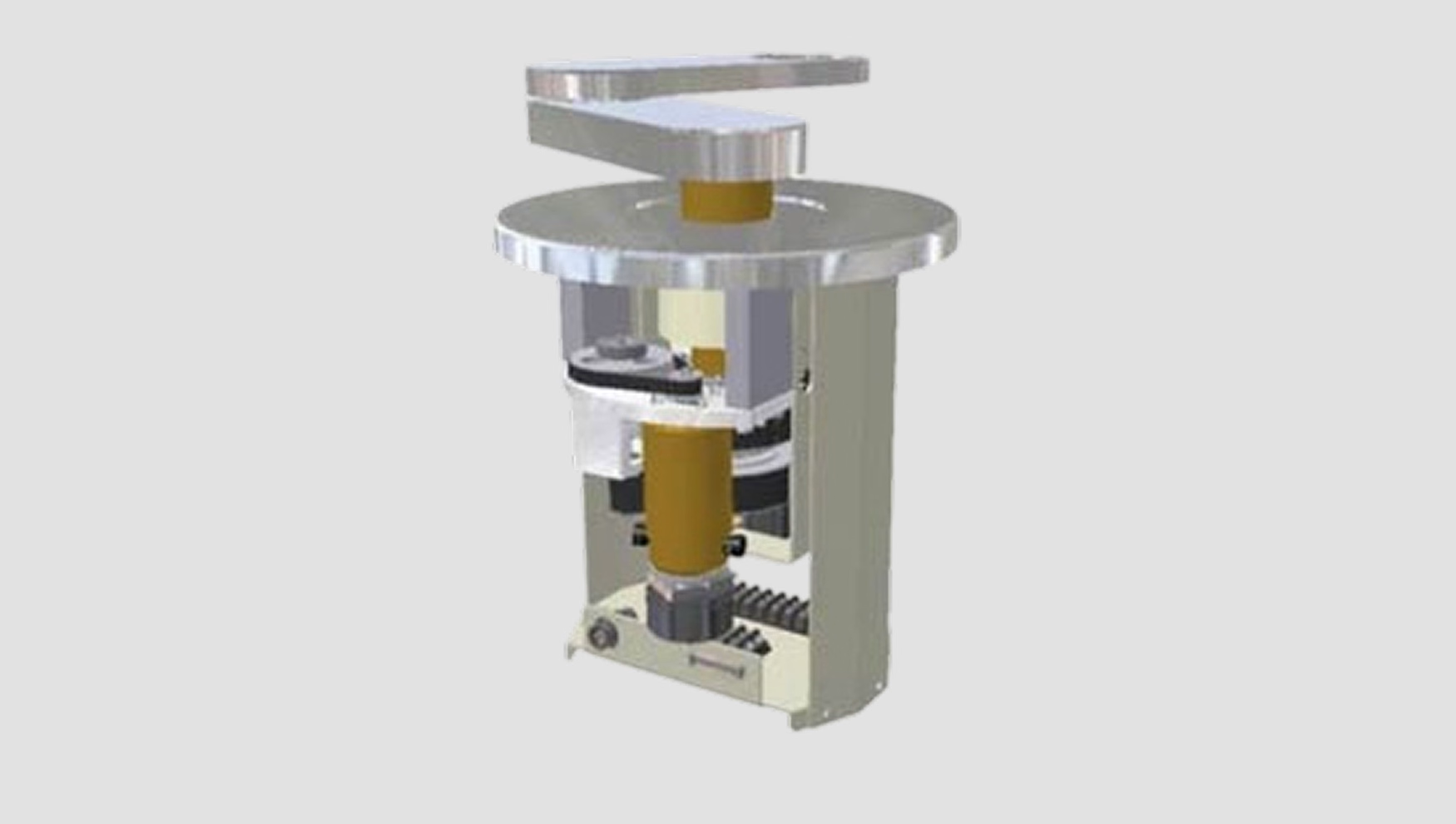
A leading semiconductor automation manufacturer needed to quickly cost reduce their vacuum robot design, which required a total redesign of the mechanisms below the mounting plate. Time was critical as an evaluation unit needed to be installed within 10 weeks. Designing for a vacuum environment posed significant challenges, including integrating a Ferrofluidic® Seal coupling to simplify power transmission, while meeting aggressive cost and lead time requirements.
Innovation
Cost-effective redesign leveraging mirrored assemblies and vendor collaboration
We delivered the first unit for evaluation within the required lead time. Key elements of the redesign included:
- Mirroring drive assemblies to increase quantities and reduce assembly time.
- Retaining the vacuum arm design from the original robot to minimize technical risk.
- Working closely with a Ferrofluidic® Seal manufacturer to modify their design to meet both cost and lead time constraints.
Result
Evaluation-ready vacuum wafer robot delivered on time and on budget
The redesigned vacuum wafer transfer robot was delivered within 10 weeks, meeting the customer’s schedule and cost targets. The approach reduced assembly complexity while maintaining reliability in the vacuum environment, enabling the customer to pursue the new revenue opportunity without delay.
Featured capabilities:
Featured sectors:
Case studies
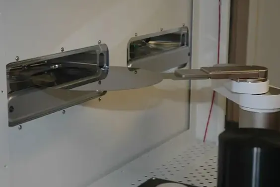
Next-generation process and device technologies demanded new measurement tools, but fabs require fully automated 300 mm configurations for evaluation. Our client needed a high-vacuum wafer automation platform…
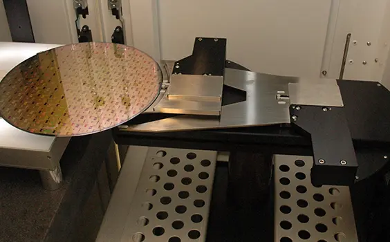
The customer needed to deliver their confocal IR laser scanning technology on a fully automated 300 mm platform. Developing in-house automation would have diverted engineering resources and delayed commercialization….
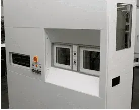
The MoCVD deposition process is critical to HBLED manufacturing, with tightly constrained carrier pockets and strict no-contact requirements on both wafer sides. Manual loading could not meet throughput…