Maximizing throughput with advanced single wafer cleaning automation
Project snapshot
Client:
Location:
Sector:
Product type:

Challenge
Maximize throughput while protecting delicate 65 nm structures
Wet cleaning remains one of the few batch processes in the modern fab. The client had developed a single wafer cleaning process for low-K materials and delicate structures that are highly sensitive to damage. They required a wafer handling system that would leverage their advanced cleaning chamber, deliver outstanding throughput, and fit within a compact footprint.
Innovation
Optimized wafer handling and system architecture
We evaluated multiple architectures and component options to optimize performance, cost, and footprint:
- Simulated system performance with several automation suppliers to identify the best configuration.
- Developed custom wafer handling mechanisms to interface with the cleaning chamber.
- Engineered the full system layout including frame, power, and facility integration.
- Collaborated closely with the client’s process engineers to ensure process integrity.
Result
Market success and industry recognition
The system was successfully introduced to the market and recognized as a “Top Ten” product of the year by a leading semiconductor industry trade group.
Featured capabilities:
Featured sectors:
Case studies
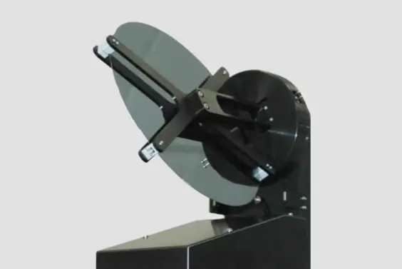
Backside contamination inspection and other process advancements require wafers to be loaded into process or inspection chambers in a 90° or 180° flipped orientation. Adding a wrist to a robot can meet…

Manual handling of polysilicon rods caused yield loss due to breakage and contamination. Rod diameters varied widely and spacing was tight, creating a mechanical challenge. The manufacturing environment…
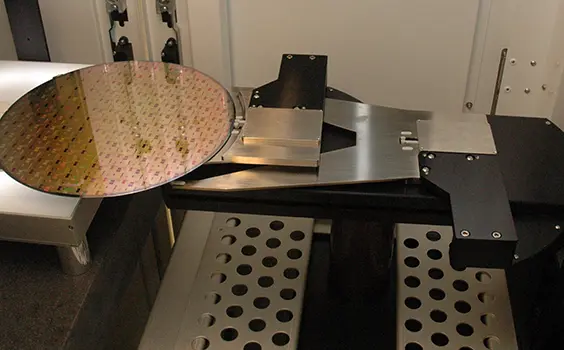
The customer needed to deliver their confocal IR laser scanning technology on a fully automated 300 mm platform. Developing in-house automation would have diverted engineering resources and delayed commercialization….