Scaled electron-beam metrology tools into fab-ready semiconductor systems
Project snapshot
Client:
Location:
Sector:
Product type:
Challenge
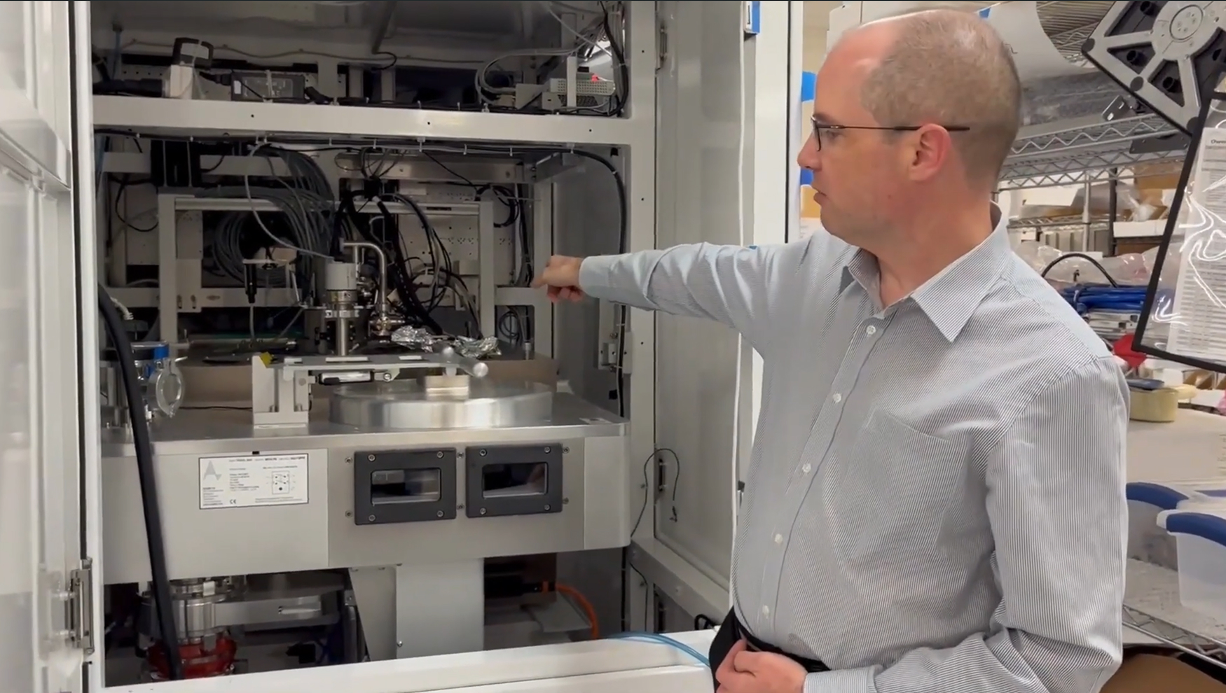
Transform a lab-based e-beam tool into a production-ready semiconductor system
Attolight, a European startup, needed to rapidly scale their electron-beam lab tool into a semiconductor fab-ready system to meet customer requirements. The project presented multiple challenges:
- The e-beam tool required high-vacuum operation, sub-micron positioning, and strict vibration control, all of which become significantly more complex at full system scale.
- The system needed to align with fab requirements for uptime, maintainability, and safety, which were not part of the original prototype design.
- The startup lacked in-house tool development and productization capabilities.
- No other single European supplier could provide a complete solution of end-to-end system development, knowledge of semiconductor fab requirements and manufacturing.
Innovation
Converting a prototype into a fab-ready, production-capable system
AIR partnered with Attolight to transform their lab prototype into a fully integrated, industry-compatible system focusing on system architecture, integration and manufacturability. Our approach included:
- Designing a high-vacuum system with e-beam compatible staging to achieve the required positional accuracy and throughput under production conditions.
- Integrating active vibration isolation tuned for system-level dynamics enabling measurement stability while supporting high acceleration.
- Establishing configuration management and reliability processes early, enabling a transition from prototype to repeatable, scalable production
- Supporting ongoing production and demonstration needs, including maintaining a demonstration system at our Silicon Valley facility.
- Worked as an extension of Attolight’s team, enabling fast decision-making and continuous alignment between performance goals and system constraints.
Result
Fab-ready e-beam systems delivered in record time
Within nine months, Attolight had an industry-compatible, production-ready e-beam system. The system met customer requirements for high-speed, high-precision metrology while reducing the burden on Attolight’s internal team.
This enabled Attolight to accelerate customer demonstrations, expand production capability, and deploy advanced metrology solutions in semiconductor fabs with reduced internal development burden and operational advantages.
Featured capabilities:
Featured sectors:
Case studies
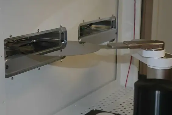
Next-generation process and device technologies demanded new measurement tools, but fabs require fully automated 300 mm configurations for evaluation. Our client needed a high-vacuum wafer automation platform…
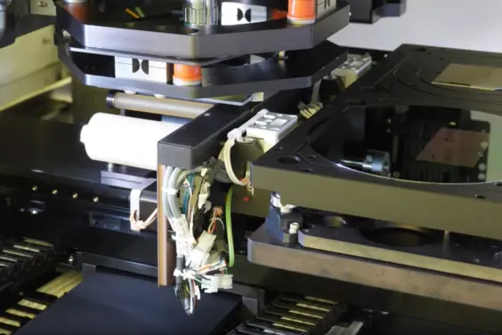
X Display Company (XDC) develops cutting-edge Micro-Transfer Printing (µTP) tools for R&D and industrial-scale manufacturing of photonics, LIDAR, lighting, and microLED display components.
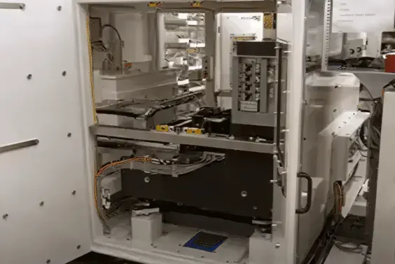
Semiconductor startup Silicon Valley X-Ray (SVXR) had proven its X-ray inspection technology on a laboratory tool and needed to rapidly deliver a production-worthy system for installation in a customer…